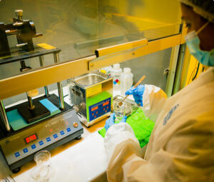
Laboratory resources
![]()
Safety Certification
Laboratory Safety is essential to prevent accidents, protect health, and ensure the accuracy of experiments. Proper safety protocols minimize exposure to hazardous chemicals and equipment-related risks. A strong safety culture fosters a secure and efficient research environment, safeguarding both personnel and scientific integrity. Our laboratory is certified by the Safe Laboratory Program of the Pontifical Catholic University of Chile and has the seal of safe practices.
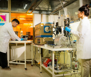
Chemical Vapor Deposition (CVD) Reactor
Description: Sed ut perspiciatis unde omnis iste natus error sit voluptatem accusantium doloremque laudantium, totam rem aperiam, eaque ipsa quae ab illo inventore veritatis et quasi architecto beatae vitae dicta sunt explicabo. Nemo enim ipsam voluptatem quia voluptas sit aspernatur aut odit aut fugit, sed quia consequuntur magni dolores eos qui ratione voluptatem sequi nesciunt.
Applications: Sed ut perspiciatis unde omnis iste natus error sit voluptatem accusantium doloremque laudantium.
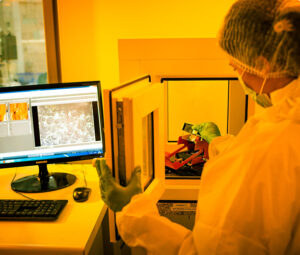
AFM (Atomic Force Microscope)
Description: An AFM is a high-resolution instrument that provides three-dimensional images of a sample's surface at the nanometric scale. It uses an extremely sharp tip attached to a cantilever to sense the forces between the tip and the sample, thus generating detailed topography.
Applications: Atomic-level material study, surface characterization, intermolecular force measurement, molecular biology, nanotechnology.
Our NaioAFM is a versatile and user-friendly atomic force microscope that allows topographic characterizations in various operating modes and performs basic electrical characterization and force spectroscopy. It uses a high-tech probe called a cantilever to measure topography and obtain 3D images of the sample’s surface at a nanometric scale.
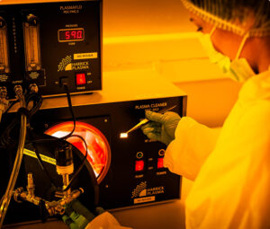
Plasma Cleaner
Description: A plasma cleaner uses low-pressure plasma to clean and activate surfaces. The plasma generates reactive species that remove organic and inorganic contaminants, improving material adhesion in subsequent processes.
Applications: Sample preparation for microscopy, cleaning substrates before thin film deposition, improving adhesion in microfabrication.
Maskless Photolithography Device
Description: A homemask device is equipment designed for the application of facial masks, usually for cosmetic or therapeutic purposes. It may include features such as heating, vibration, or LED light to enhance the effects of the applied products.
Applications: Skincare, light therapy, facial relaxation.
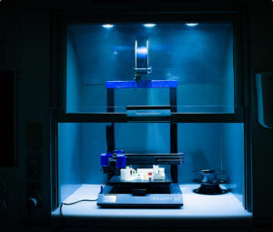
3D Printer
Description: A 3D printer creates three-dimensional objects from a digital model. It deposits material in successive layers to form the final piece. Different 3D printing technologies include FDM (Fused Deposition Modeling), SLA (Stereolithography), and SLS (Selective Laser Sintering).
Applications: Rapid prototyping, custom part manufacturing, complex structure modeling, bio-printing.
Metalizer
Description: A metalizer deposits a thin layer of metal onto a surface. Metalization methods can include thermal evaporation, sputtering, or electrodeposition.
Applications: Electronics manufacturing, decorative coatings, electrical conductivity enhancement, corrosion protection.
Mass Spectrometer
A Residual Gas Analyzer (RGA) is a device used to detect and analyze the relative pressure of different gases in a vacuum system, allowing the estimation of relative concentration of molecular and atomic species at the parts per billion (PPB) resolution.
Applications: It is commonly used in industries like semiconductor manufacturing, aerospace, and research laboratories to monitor gas impurities and ensure the integrity of vacuum environments.
Spin Coater
Description: A spin coater deposits a uniform liquid layer onto a rotating substrate. The rotation speed and liquid viscosity determine the final layer thickness.
Applications: Semiconductor device fabrication, optical coatings, sample preparation for microscopy.
Dip Coater
Description: A dip coater immerses a substrate into a liquid bath to coat it uniformly. The immersion and extraction speed, as well as liquid viscosity, influence the layer thickness.
Applications: Thin film manufacturing, protective coatings, sample preparation for analysis.
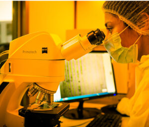
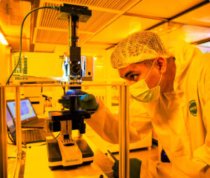
Optical Microscope
Description: An optical microscope uses lenses to magnify an image of a small object. It allows the observation of biological samples, materials, and structures at the cellular level.
Applications: Biology, medicine, materials science, quality control.
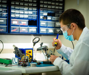
Electronic Work Area
Description: An electronic work area is a space equipped with specialized tools and equipment for designing, manufacturing, and testing electronic circuits. It may include soldering stations, oscilloscopes, power supplies, and design software.
Applications: Electronic prototype development, equipment repair, electronics research.